
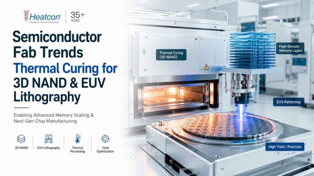
What Are The Latest Trends In Semiconductor Fab Thermal Curing?
The semiconductor industry is advancing at a rapid pace, with global sales surpassing $600 billion in 2023 according to the Semiconductor Industry Association. At the forefront of this evolution are two key processes: thermal curing for 3D NAND and EUV lithography. These technologies are fundamentally redefining memory density, device performance, and production efficiency.
As chipmakers worldwide race to innovate, the role of precise thermal management has become more critical than ever. The intricate requirements of advanced fabrication demand equipment and sensors that can deliver uncompromising accuracy and reliability. That’s where Heatcon Sensors, a leader in custom temperature sensor solutions and heat-generating equipment, becomes a pivotal partner for semiconductor fabs across India, the US, UAE, Indonesia, Germany, South Korea, Saudi Arabia, Russia, Bahrain, Kuwait, and beyond.
Why Is Thermal Curing Essential For 3D NAND Manufacturing?
Thermal curing is a cornerstone in the production of 3D NAND memory, a technology that stacks memory cells vertically to exponentially increase storage capacity. Without precise thermal management, the integrity of these multi-layer stacks would be compromised, leading to poor device performance and reduced yields.
- 3D NAND curing involves carefully controlled heating cycles that activate chemical processes, cure dielectrics, and stabilize interconnects across dozens or even hundreds of layers.
- Any thermal deviation can cause layer misalignment, stress fractures, or incomplete material transformation, severely impacting device reliability.
Heatcon Sensors designs and manufactures custom temperature sensors—such as RTDs and thermocouples—specifically calibrated for 3D NAND curing processes. These sensors enable fabs to maintain the stringent thermal profiles required for successful vertical NAND integration, whether deployed in a high-capacity semiconductor cleanroom oven or a specialized furnace.
How Does EUV Lithography Revolutionize Advanced Fabrication?
EUV lithography stands at the leading edge of advanced fabrication, allowing the semiconductor industry to etch circuit patterns at the sub-7nm scale with extreme precision. This technology employs extreme ultraviolet light with a wavelength of just 13.5 nm, enabling the production of next-generation logic and memory chips.
- The success of EUV lithography hinges on ultra-clean environments and precise thermal control to prevent defects and achieve the required critical dimensions.
- Advanced temperature sensors from Heatcon Sensors ensure that the photomasks, wafer stages, and resist layers are maintained within optimal temperature windows—minimizing distortion and maximizing yield.
As the race to smaller nodes intensifies, fabs in regions like South Korea, Germany, and the US are increasingly relying on sophisticated sensor arrays and robust heating systems to support EUV toolsets. Heatcon Sensors offers not only sensors but also heat-generating equipment like high density cartridge heaters, electric furnaces, and hot air blowers—key enablers for state-of-the-art lithography suites.
What Is The Role Of Semiconductor Cleanroom Oven In Fabrication?
A semiconductor cleanroom oven is indispensable in both wafer processing and packaging stages. These ovens control the environment’s temperature, humidity, and particle levels—ensuring that sensitive materials are processed without contamination.
- Precision heating enables consistent curing, annealing, and sintering of semiconductor materials.
- Integration with custom temperature sensors from Heatcon Sensors provides real-time feedback, alerting operators to fluctuations and enabling immediate corrective action.
Heatcon Sensors customizes and supplies semiconductor cleanroom oven solutions and temperature control systems to fabs and research facilities globally. Their expertise guarantees that every oven meets the exacting standards of advanced fabrication, supporting the world’s most complex chip designs.
How Can Heatcon Sensors Support Global Fabs With Custom Solutions?
Heatcon Sensors is known for its commitment to quality and customization. The company’s range of products includes:
- RTDs and thermocouples tailored for semiconductor processing
- High density cartridge heaters
- Electric furnaces for wafer annealing and curing
- Hot air blowers for cleanroom applications
- Ovens and custom heating systems for labs and fabs
Every product is engineered for reliability and accuracy, crucial for 3D NAND curing and EUV lithography. Heatcon Sensors supplies equipment and sensors not only across India but also to the US, UAE, Indonesia, Germany, South Korea, Saudi Arabia, Russia, Bahrain, Kuwait, and every major semiconductor hub worldwide.
Customers can reach out for custom requirements by submitting their information via the contact form, through WhatsApp on the website, or by calling +91 9164833027 / +91 9844233244 for immediate assistance.
What Are The Benefits Of Partnering With Heatcon Sensors?
Choosing Heatcon Sensors means gaining a technology partner who understands the nuances of semiconductor manufacturing:
- Expertise: Decades of experience in designing for advanced fabrication processes.
- Customization: Solutions tailored for your unique process requirements, from sensor calibration to equipment architecture.
- Global Reach: Seamless delivery and support across continents and cities, including remote and high-tech locations.
- Reliability: Robust, quality-tested sensors and heating equipment that reduce downtime and enhance process yields.
By overlooking the importance of high-precision thermal management, fabs risk lower yields, higher defect rates, and missed opportunities in a fiercely competitive market. Don’t let outdated sensors or generic equipment hold you back—partner with Heatcon Sensors for a future-ready semiconductor operation.
How To Implement Advanced Fabrication With The Right Heat Solutions?
Implementing advanced fabrication demands not only high-spec process tools but also support infrastructure that can keep pace. Whether you are setting up a new facility or upgrading an existing fab, consider the following steps:
- Assess Your Process Needs: Identify where precise temperature control is critical—such as 3D NAND curing, EUV lithography, or specialty wafer annealing.
- Engage With Experts: Consult with Heatcon Sensors for a custom assessment and proposal, factoring in your unique cleanroom and equipment constraints.
- Integrate And Monitor: Deploy Heatcon Sensors’ RTDs, thermocouples, and heat-generating devices, then monitor performance with real-time data analytics.
- Scale Globally: Leverage Heatcon’s worldwide supply capabilities to ensure consistent standards across multi-national fab sites—whether in India, the US, Germany, or the Middle East.
Advanced fabrication is only as robust as its weakest process link. Don’t compromise—choose a partner who delivers performance, reliability, and global reach.
About Heatcon Sensors
Heatcon Sensors is a premier manufacturer of customized RTDs, thermocouples, and temperature sensors for industrial and semiconductor applications. With expertise in designing and building heat-generating equipment—including semiconductor cleanroom oven, electric furnaces, hot air blowers, and high density cartridge heaters—Heatcon Sensors supports clients in India and around the globe.
The company’s commitment to innovation, quality, and customer satisfaction makes it the trusted partner for advanced fabrication plants, research centers, and semiconductor manufacturers navigating the rapidly evolving landscape of 3D NAND curing and EUV lithography.
Don’t let your fab fall behind. Contact Heatcon Sensors today via the online form, WhatsApp interface, or call directly at +91 9164833027 or +91 9844233244 for immediate solutions tailored to your requirements.
Frequently Asked Questions
What are the latest trends in thermal curing for 3D NAND fabrication?
The latest trends in thermal curing for 3D NAND fabrication emphasize ultra-uniform temperature control, contamination-free environments, and precise ramp/soak profiles to optimize device reliability and stack integrity. As the number of layers in 3D NAND increases, advanced fabrication demands higher process repeatability and tighter control over thermal budgets. Heatcon Sensors addresses these needs with specialized sensor solutions that integrate seamlessly into a semiconductor cleanroom oven environment, ensuring exceptional accuracy and stability during the 3D NAND curing process.
How does EUV lithography impact temperature sensing requirements in fabs?
EUV lithography introduces stringent requirements for thermal uniformity and cleanliness due to its sensitivity to temperature-induced distortions and contamination. Accurate temperature monitoring within lithography tools and associated bake chambers is essential to prevent overlay errors and maintain critical dimension control. Heatcon Sensors supplies precision sensors capable of withstanding the high-vacuum, low-contamination settings required for EUV lithography, supporting the advanced fabrication processes found in today’s leading-edge fabs.
Why is a semiconductor cleanroom oven crucial for advanced device manufacturing?
A semiconductor cleanroom oven is vital for processes like curing, annealing, and polymerization, where even minute particle contamination or temperature deviations can lead to device failure. These ovens are engineered for ultra-clean operation and tight thermal control. Heatcon Sensors’ temperature and process sensors are specifically designed to maintain accuracy and repeatability in these environments, helping manufacturers meet the quality standards required for high-yield advanced fabrication.
What challenges does 3D NAND curing present, and how does Heatcon Sensors help?
3D NAND curing processes involve multiple layers and complex structures, making uniform heat distribution and contamination control especially challenging. Variations in temperature can affect layer adhesion and electrical performance. Heatcon Sensors offers robust, high-accuracy sensors and integrated assemblies that withstand harsh chemistries and fluctuating temperatures, ensuring reliable monitoring and control during 3D NAND curing stages.
How do Heatcon Sensors’ solutions integrate with EUV lithography tools?
Heatcon Sensors provides temperature sensors and assemblies engineered for the exacting requirements of EUV lithography, including high-purity, vacuum-compatible materials and custom form factors for precise placement within tool chambers. These solutions help maintain the narrow process windows and thermal stability critical for achieving sub-7nm patterning in advanced fabrication environments.
What types of temperature sensors are best suited for semiconductor cleanroom ovens?
For semiconductor cleanroom oven applications, resistance temperature detectors (RTDs), thermocouples, and thermistors with contamination-resistant sheathing and precision calibration are ideal. Heatcon Sensors offers a wide range of these sensors, specifically designed for cleanroom compatibility and tight thermal tolerances, to suit varying process needs in advanced device manufacturing.
Can Heatcon Sensors support custom sensor requirements for new process tools?
Absolutely. Heatcon Sensors specializes in collaborating with semiconductor OEMs and fabs to design and manufacture custom sensor assemblies tailored to unique process conditions—whether for new EUV lithography platforms, 3D NAND curing ovens, or other advanced fabrication tools. This includes rapid prototyping, cleanroom packaging, and compliance with industry-specific standards.
What are the primary benefits of using Heatcon Sensors in advanced fabrication environments?
Key benefits include reliable operation in harsh and ultra-clean environments, high measurement accuracy, robust build quality, and support for custom integration. These attributes help fabs optimize process yields, reduce downtime, and ensure process repeatability for critical steps such as 3D NAND curing and EUV lithography.
How does precise temperature control improve outcomes in 3D NAND and EUV processes?
Precise temperature control ensures uniform layer formation, reduces defects, and enables tighter critical dimension tolerances, directly impacting device performance and yield. In both 3D NAND curing and EUV lithography, Heatcon Sensors’ solutions deliver the accuracy and reliability required to meet these demanding process specifications.